
1.No output signal is detected from the crystal
1-1. Crystal Signal Verification
To validate the functionality of the crystal, utilize an oscilloscope or frequency counter to assess the signal output from its terminals. Should there be no detectable signal, proceed systematically from step 1-1 through 1-4 to troubleshoot the issue. Conversely, if you observe a signal emerging from the crystal's output terminal (Xout) yet none from the input terminal (Xin), proceed with steps 1-5 through 1-6 for a detailed inspection of the crystal.
1-2. Crystal Performance Evaluation
To ensure the crystal is performing as intended, it is essential to decouple it from the system and subject it to a rigorous performance check using a specialized testing device. This will provide insight into its frequency accuracy and load capacitance, ensuring they align with your specified requirements. Additionally, you may opt to engage your supplier's services for a comprehensive analysis.
1-3. Addressing Irregularities
In the event that the crystal fails to resonate, its load capacitance deviates from your specifications, or there exists a significant discrepancy between its current frequency and your targeted value, it is advisable to dispatch the crystal to your supplier for a thorough quality analysis. However, if the frequency and load capacitance adhere to your standards, further evaluation through an equivalent circuit test becomes necessary.
1-4. Conducting an Equivalent Circuit Analysis
1-4-1. Oscillation Circuit Fundamentals
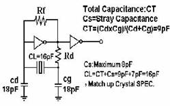
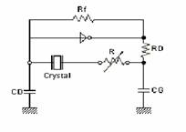
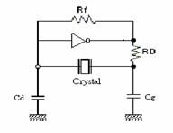
The fundamental architecture of a microprocessor's oscillation circuit often aligns with the principles of the Colpitts circuit. Within this configuration, Cd and Cg represent the external load capacitors, typically integrated into the chipset itself. (For reference, consult the chipset's technical specifications.) Rf, the feedback resistance, typically ranges from 200KΩ to 1MΩ and is commonly embedded within the chipset. Meanwhile, Rd, the limiting resistor, typically ranges from 470Ω to 1KΩ and is only necessary in circuits with high-voltage supplies.
1-4-2. Ensuring Stable Oscillation
A crucial aspect of maintaining a stable oscillation circuit is the presence of a negative resistance. The value of this negative resistance must exceed five times the resistance of the crystal to ensure stability. Mathematically, this can be expressed as |-R| > 5 × Rr. For instance, if the crystal resistance is 40Ω, the negative resistance of the IC should be less than -200Ω to achieve a reliable oscillation circuit.
1-4-3. The Significance of Negative Resistance
The concept of "negative resistance" serves as a critical benchmark for assessing the quality of an oscillation circuit. In scenarios where the circuit may face challenges due to aging, thermal variations, voltage fluctuations, or other factors, a low "Q" value could lead to oscillation failure. Therefore, it is imperative to accurately measure the negative resistance (-R) of the circuit, following the recommended procedures outlined below:
To troubleshoot an oscillation circuit's stability, several key steps must be taken into account:
1-4-4 Connecting and Testing Resistance (R)
The first step involves connecting the resistance (R) in series with the crystal. Adjust R's value from the oscillation's onset to its cessation. Measure R's value precisely during oscillation. This will allow you to calculate the negative resistance using the formula: |–R| = R + Rr, where Rr is the crystal's resistance.
Note: Keep in mind that stray capacitance within the circuit can potentially impact the measured values.
1-4-5 Troubleshooting Unstable Oscillation
If the crystal's parameters are within normal range but the oscillation circuit fails to operate consistently, there may be an issue with the IC's resistance value. Here are three methods to address this issue:
Reduce the values of the external capacitors (Cd and Cg) and opt for a crystal with a lower load capacitance (CL).
Select a crystal with a lower resistance (Rr).
Measure R's value during oscillation and adjust Cd and Cg unequally. Specifically, increasing Cd (Xout) while reducing Cg (Xin) can enhance the amplitude of the waveform output from Xin, which is often used in subsequent circuits.
1-5 Addressing High Power Consumption in Backend Circuits
When there is a signal output from Xout but not from Xin, it suggests that the backend circuit's power consumption is excessively high. To mitigate this, a buffer can be introduced between the circuit's output and its rear electrode to enhance driving capabilities for the backend circuit.
1-6 Further Assistance
If the problem persists after following the methods outlined in 1-4-4, you can consider contacting field application engineers from crystal or IC manufacturers for expert guidance. They can provide tailored solutions based on your specific circuit configuration and requirements.
2.The system's malfunction is attributed to the insufficient amplitude of the output waveform generated by the crystal oscillator, affecting its overall operational efficiency
2-1. Please conduct measurements on the signals from the crystal's two terminals utilizing either an Oscilloscope or a Frequency Counter. If the Frequency falls outside the specified range and its output waveform amplitude is insufficient (e.g., exceeding ±200ppm), proceed to steps 2-3 through 2-5 accordingly.
2-2. The equation for determining the relationship between Capacitances and Frequency is outlined as follows:
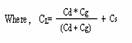
FL = FR * ( 1 + C1 / 2 * ( C0 + CL) ) where
The graph depicts the correlation between capacitance variations and changes in frequency (known as frequency pullability):
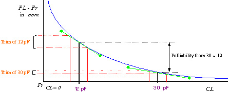
If the frequency recorded by the Frequency Counter exceeds the desired target, it is recommended to increase the capacitance values (CL, or Cd and Cg) to reduce the frequency and align it with the target. Conversely, if the frequency is too low, reducing the capacitance values will raise the frequency.
After making adjustments to the frequency, it is crucial to verify if the waveform amplitude has improved. If there is an improvement, it suggests that the initial circuit design was not tuned to the crystal's optimal resonant point. With the appropriate adjustments to the resonant point, the crystal should operate normally.
2-3. If the waveform amplitude remains unimproved despite the frequency being close to the target, you can enhance it using the following three methods:
Method 1: Reduce the value of external capacitances (Cd and Cg) and select a crystal with a lower load capacitance (CL).
Method 2: Employ a crystal with a lower resistance (Rr).
Method 3: Implement a design with unequal values for Cd and Cg. Specifically, increase the load capacitance of Cd (Xout) and decrease the load capacitance of Cg (Xin) to boost the output waveform amplitude at Xin, which will be utilized in the subsequent circuitry.
We recommend utilizing these methods to optimize costs while ensuring reliability and safety.
2-4. After improving the waveform amplitude, utilize the Frequency Counter to verify that the adjusted frequency still adheres to the original specifications. If the frequency falls outside the specified range, it is advisable to select a crystal with an appropriate CL value based on your target frequency.
2-5. If the frequency is significantly higher than the target, consider adopting a crystal with a lower CL value. Conversely, if the frequency is too low, opt for a crystal with a higher CL value.
3.The system malfunction is attributed to the excessive deviation of the frequency output, exceeding the permissible limits
3-1. To address the issue of excessive deviation in frequency output, we can employ the following methods:
Method 1: Adjust the values of external capacitances, Cd, and Cg. If the frequency measured by the Frequency Counter exceeds the target, increasing the external capacitance, CL (or the values of Cd and Cg), will lower the frequency towards the target. Conversely, if the frequency is too low, reducing the capacitance values will increase the frequency.
Method 2: Utilize a crystal with a different capacitance value (CL). If the frequency is significantly higher than the target, adopting a crystal with a lower capacitance is recommended. Conversely, for a frequency that is too low, a crystal with a higher capacitance should be used.
3-2. After adopting the correct capacitance and adjusting the frequency to the target, it is crucial to verify the waveform amplitude using an Oscilloscope. If the waveform amplitude diminishes due to the addition of external capacitances, consider employing Method 2 to adjust the frequency by reducing the external capacitances and selecting a crystal with a lower capacitance.
4.The frequency output is currently at only one-third of the desired target frequency
4-1. Depicted below is a graph highlighting the resistance traits of a crystal:
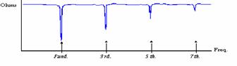
Crystals possess numerous vibrational patterns, ranging from the Fundamental to the 3rd, 5th, and subsequent overtones. The resistance of a crystal reaches its nadir when the Fundamental mode is activated, facilitating effortless oscillation. Conversely, for the 3rd overtone mode, a magnifying circuit is imperative to suppress the fundamental mode's frequency feedback, ensuring it remains inferior to the 3rd overtone's. Thus, encountering a frequency that's a mere third of the desired target should prompt an inspection of the magnifying circuit's presence and calibration, as the circuit environment may cater more to the Fundamental mode than the 3rd overtone.
4-2. In the absence of a magnifying circuit or inadequate settings, the circuitry might fail to achieve oscillation.
4-3. Below are the distinct applications of the Fundamental and 3rd Overtone modes:
a. Utilizing the Fundamental mode
b. Leveraging the 3rd Overtone mode
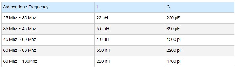
4-4. The subsequent table outlines the optimal L and C values for the 3rd Overtone mode across various frequencies:
5.The frequency output triples the target, indicating deviation
5-1. Although unlikely, please verify if the frequency feedback of the third-tone mode exceeds the fundamental mode due to the magnifying circuit. This issue could arise if the magnifying circuit is integrated into the chipset. To address it, we recommend utilizing a crystal designed for third-tone mode.
5-2. Additionally, a poorly designed magnifying circuit for the third-tone mode may result in the circuit oscillating at the fifth-tone mode or failing to oscillate altogether.
6.System malfunction occurs when the output waveform amplitude exceeds the permissible limit
6-1.To troubleshoot the issue, please follow the resolution for scenario 2 by augmenting the capacitance at the Xin terminal and subsequently verifying if there's an improvement in the waveform amplitude.
7.System malfunction or display distortion occurs on the monitor when the output waveform is disrupted by external signal interference
7-1. Utilize a Spectrum Analyzer to identify the frequencies of interfering signals. This will help us pinpoint the underlying issues based on the detected frequencies.
7-2. If the interference stems from an AC signal from the power supply, ensure that both the power supply and signal grounds are in a floating state. If not, please adjust them accordingly.
7-3. For high-frequency interference, consider the following solutions:
- Utilize the crystal's case as a grounding point.
- Select a crystal with a smaller C0 value.
- Increase the external circuit capacitances Cd and Cg, and opt for a crystal with a higher load capacitance CL.
7-4. If the aforementioned methods fail to resolve the issue, inspect the surrounding circuits and PCB layout. If both are in order, it is advisable to consult the IC manufacturer to investigate how the chipset design reacts to unknown signals. Altering the design of surrounding circuits may only mitigate the problem rather than providing a complete solution. Typically, identifying and rectifying the issue within the chipset design offers the most effective solution.
8.The EMI of the circuit is excessive
The resolutions for this EMI issue are similar to those for problem 7. Kindly refer to steps 7-1 through 7-4 for guidance.
9.The crystal fails to oscillate upon installation on the PCB
9-1. Utilize an Oscilloscope or Frequency Counter to assess the signals from the crystal's terminals. Follow steps 9-1 to 9-4 for testing. If Xin produces a signal with low waveform amplitude, refer to steps 2-1 through 2-5.
9-2. Remove the crystal and use a professional testing machine to verify its frequency and load capacitance. Ensure they resonate and meet your requirements. Alternatively, have your supplier conduct the tests.
9-3. If issues arise, such as no vibration, incorrect load capacitance, or a significant deviation from the target frequency, submit the crystal to your supplier for Quality Analysis.
9-4. If the frequency and load capacitance align with your specifications, and the crystal passes the DLD test, proceed with an Equivalent Circuit Test. Refer to steps 1-4 through 1-6.
9-5. Should the crystal fail the DLD test, forward it to your supplier for Quality Analysis to identify further improvements.
10.The crystal malfunctions or experiences frequency shifts during thermal testing on the PCB
10-1. Remove the crystal and use a thermal testing machine to verify its frequency and resistance. Ensure it oscillates within specifications. Alternatively, have your crystal supplier conduct the tests. (Note: Thermal test points should be spaced at least 10℃ apart.)
10-2. If the crystal's resistance or frequency falls outside specifications within the operating temperature range, please send it to the manufacturer for Quality Analysis and potential improvements.
10-3. Assuming the crystal passes the thermal test, scrutinize the oscillation circuit and characteristics of other components, including the temperature coefficient of external capacitance and chip circuit.
11.The crystal exhibits insufficient frequency pullability or asymmetrical frequency variations
11-1.As depicted, there is an inverse relationship between the capacitance of the VCXO circuit and its pullability, implying that a decrease in capacitance leads to a wider frequency pulling range (FL-Fr), and vice versa. Given that the VCXO circuit's capacitance is regulated by a varistor, we can enhance the frequency pulling range by utilizing a varistor with reduced capacitance or a broader adjustment range.
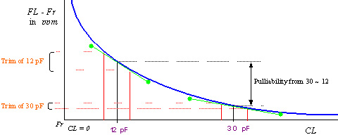
11-2. Beyond external circuit adjustments, the crystal's parameters also influence the frequency pulling range. Key reference parameters include Trim Sensitivity (TS), C0/C1(r), C1, C0, and so on. The relationships between these parameters and frequency pullability are outlined below:
C0↑ , C1↑, C0/C1(r)↓ , TS↑ , pullability ↑
11-3. If the frequency pulling range is insufficient, we can modify the crystal's specifications to achieve the desired range.
11-4. When one side of the pulling range is inadequate while the other is excessive, resulting in an asymmetric pulling range, we can adjust the crystal's load capacitance (CL) to achieve symmetry and adequate pulling on both sides.
12.The crystal exhibits excessive frequency deviation over time or significant sensitivity to stray capacitance once installed on the PCB
12-1. Given the crystal pull ability curve shown in 11-1, reduced capacitance leads to greater frequency changes. If the frequency distribution is excessively wide, consider the following approaches:
- Increase the values of Cd and Cg capacitances and select a crystal with a higher load capacitance (CL).
- Utilize more precise capacitors for Cd and Cg (with minimal capacitance variation).
- Employ a more stable crystal (with minimal frequency variation).
12-2. Additionally, if the frequency distribution cannot be optimized to meet specifications due to significant stray capacitance on the PCB, it may necessitate a new layout design based on identifying and addressing the sources of stray capacitance.